- 您现在的位置:买卖IC网 > Sheet目录1994 > DS1743P-70+ (Maxim Integrated Products)IC RTC RAM Y2K 5V 70NS 34-PCM
DS1743/DS1743P Y2K-Compliant, Nonvolatile Timekeeping RAMs
3 of 17
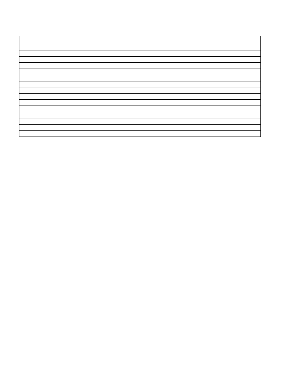
ORDERING INFORMATION
PART
TEMP RANGE PIN-PACKAGE
VOLTAGE
(V)
TOP MARK**
DS1743-85+
0°C to +70°C
28 EDIP Module
5
DS1743-85
DS1743-100+
0°C to +70°C
28 EDIP Module
5
DS1743-100
DS1743-100 IND+
-40°C to +85°C
28 EDIP Module
5
DS1743-100-IND
DS1743P-85+
0°C to +70°C
34 PowerCap*
5
DS1743P-85
DS1743P-100+
0°C to +70°C
34 PowerCap*
5
DS1743P-100
DS1743P-100IND+
-40°C to +85°C
34 PowerCap*
5
DS1743P-100 IND
DS1743W-120+
0°C to +70°C
28 EDIP Module
3.3
DS1743W-120
DS1743W-120 IND+
-40°C to +85°C
28 EDIP Module
3.3
DS1743W-120 IND
DS1743W-150+
0°C to +70°C
28 EDIP Module
3.3
DS1743W-150
DS1743W-150 IND+
-40°C to +85°C
28 EDIP Module
3.3
DS1743W-150 IND
DS1743WP-120+
0°C to +70°C
34 PowerCap*
3.3
DS1743WP-120
DS1743WP-120 IND+
-40°C to +85°C
34 PowerCap*
3.3
DS1743WP-120 IND
DS9034PCX+
0°C to +70°C
PowerCap
—
DS9034PC
DS9034I-PCX+
-40°C to +85°C
PowerCap IND
—
DS9034PCI
+Denotes a lead(Pb)-free/RoHS-compliant package.
*DS9034PCX+ or DS9034I-PCX+ required (must be ordered separately).
**A ‘+’ indicates lead(Pb)-free. The top mark will include a ‘+’ symbol on lead(Pb)-free devices.
DESCRIPTION
The DS1743 is a full-function, year-2000-compliant (Y2KC), real-time clock/calendar (RTC) and 8k x 8
nonvolatile static RAM. User access to all registers within the DS1743 is accomplished with a bytewide
interface as shown in Figure 1. The RTC information and control bits reside in the eight uppermost RAM
locations. The RTC registers contain century, year, month, date, day, hours, minutes, and seconds data in
24-hour binary-coded decimal (BCD) format. Corrections for the day of the month and leap year are made
automatically. The RTC clock registers are double buffered to avoid access of incorrect data that can occur
during clock update cycles. The double-buffered system also prevents time loss as the timekeeping
countdown continues unabated by access to time register data. The DS1743 also contains its own power-
fail circuitry, which deselects the device when the VCC supply is in an out-of-tolerance condition. When
VCC is above VPF, the device is fully accessible. When VCC is below VPF, the internal CE signal is forced
high, preventing any access. When VCC rises above VPF, access remains inhibited for TREC, allowing time
for the system to stabilize. These features prevent loss of data from unpredictable system operation brought
on by low VCC as errant access and update cycles are avoided.
PACKAGES
The DS1743 is available in two packages: the 28-pin DIP and the 34-pin PowerCap module. The 28-pin
DIP-style module integrates the crystal, lithium energy source, and silicon all in one package. The 34-pin
PowerCap Module Board is designed with contacts for connection to a separate PowerCap (DS9034PCX)
that contains the crystal and battery. This design allows the PowerCap to be mounted on top of the
DS1743P after the completion of the surface-mount process. Mounting the PowerCap after the surface-
mount process prevents damage to the crystal and battery due to the high temperatures required for solder
reflow. The PowerCap is keyed to prevent reverse insertion. The PowerCap Module Board and PowerCap
are ordered separately and shipped in separate containers.
发布紧急采购,3分钟左右您将得到回复。
相关PDF资料
DS1744-70IND
IC RTC RAM Y2K 5V 70NS 28-EDIP
DS1746-70IND
IC RTC RAM Y2K 5V 70NS 32-EDIP
DS1747W-120IND
IC RTC RAM Y2K 3.3V 120NS 32EDIP
DS17887-3-IND
IC RTC 3V 8K NV RAM 24-EDIP
DS1851E-010+
IC DAC DUAL NV TEMP CNTRL 8TSSOP
DS2187S+
IC RECEIVE LINE INTERFACE 20SOIC
DS21Q58L
IC TXRX E1 QUAD 3.3V 100-LQFP
DS2404B
IC ECONORAM TIMECHIP 5.5V 16SSOP
相关代理商/技术参数
DS1743P-85+
功能描述:实时时钟 Timekeeping NV RAM RoHS:否 制造商:Microchip Technology 功能:Clock, Calendar. Alarm RTC 总线接口:I2C 日期格式:DW:DM:M:Y 时间格式:HH:MM:SS RTC 存储容量:64 B 电源电压-最大:5.5 V 电源电压-最小:1.8 V 最大工作温度:+ 85 C 最小工作温度: 安装风格:Through Hole 封装 / 箱体:PDIP-8 封装:Tube
DS1743P-85IND+
功能描述:实时时钟 Timekeeping NV RAM RoHS:否 制造商:Microchip Technology 功能:Clock, Calendar. Alarm RTC 总线接口:I2C 日期格式:DW:DM:M:Y 时间格式:HH:MM:SS RTC 存储容量:64 B 电源电压-最大:5.5 V 电源电压-最小:1.8 V 最大工作温度:+ 85 C 最小工作温度: 安装风格:Through Hole 封装 / 箱体:PDIP-8 封装:Tube
DS1743P-C01+
制造商:Maxim Integrated Products 功能描述:Y2KC RAM PCAP 8KX8 100NS ROCKWELL - Trays
DS1743W-120
功能描述:实时时钟 RoHS:否 制造商:Microchip Technology 功能:Clock, Calendar. Alarm RTC 总线接口:I2C 日期格式:DW:DM:M:Y 时间格式:HH:MM:SS RTC 存储容量:64 B 电源电压-最大:5.5 V 电源电压-最小:1.8 V 最大工作温度:+ 85 C 最小工作温度: 安装风格:Through Hole 封装 / 箱体:PDIP-8 封装:Tube
DS1743W-120 IND
功能描述:实时时钟 RoHS:否 制造商:Microchip Technology 功能:Clock, Calendar. Alarm RTC 总线接口:I2C 日期格式:DW:DM:M:Y 时间格式:HH:MM:SS RTC 存储容量:64 B 电源电压-最大:5.5 V 电源电压-最小:1.8 V 最大工作温度:+ 85 C 最小工作温度: 安装风格:Through Hole 封装 / 箱体:PDIP-8 封装:Tube
DS1743W-120+
功能描述:实时时钟 Timekeeping NV RAM RoHS:否 制造商:Microchip Technology 功能:Clock, Calendar. Alarm RTC 总线接口:I2C 日期格式:DW:DM:M:Y 时间格式:HH:MM:SS RTC 存储容量:64 B 电源电压-最大:5.5 V 电源电压-最小:1.8 V 最大工作温度:+ 85 C 最小工作温度: 安装风格:Through Hole 封装 / 箱体:PDIP-8 封装:Tube
DS1743W-120IND
功能描述:实时时钟 RoHS:否 制造商:Microchip Technology 功能:Clock, Calendar. Alarm RTC 总线接口:I2C 日期格式:DW:DM:M:Y 时间格式:HH:MM:SS RTC 存储容量:64 B 电源电压-最大:5.5 V 电源电压-最小:1.8 V 最大工作温度:+ 85 C 最小工作温度: 安装风格:Through Hole 封装 / 箱体:PDIP-8 封装:Tube
DS1743W-120IND+
功能描述:实时时钟 Timekeeping NV RAM RoHS:否 制造商:Microchip Technology 功能:Clock, Calendar. Alarm RTC 总线接口:I2C 日期格式:DW:DM:M:Y 时间格式:HH:MM:SS RTC 存储容量:64 B 电源电压-最大:5.5 V 电源电压-最小:1.8 V 最大工作温度:+ 85 C 最小工作温度: 安装风格:Through Hole 封装 / 箱体:PDIP-8 封装:Tube